ACM Research shipped its first PECVD SiCN system, marking an equipment milestone for advanced chipmaking and packaging validation.
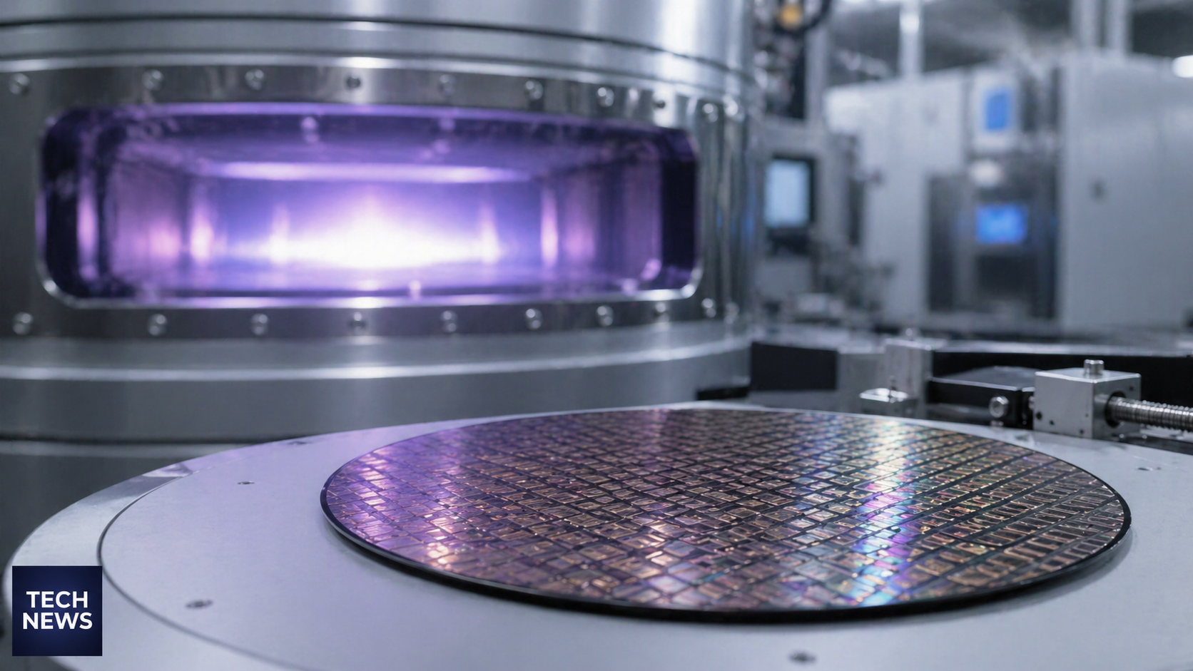
On April 27, 2026, ACM Research announced the shipment of its first plasma-enhanced chemical vapor deposition (PECVD) system designed specifically for silicon carbonitride (SiCN) deposition to a leading semiconductor manufacturer. This delivery marks a significant milestone in semiconductor equipment development, enabling advanced chipmaking processes that support smaller and more capable microchips. The system has passed ACM’s internal testing at their Lingang laboratory and is now en route to the customer’s site for validation, a crucial step before it can be qualified for production use.
This development is important beyond the chip industry because it underlines the critical role specialized manufacturing tools play in the electronics supply chain. Achieving extreme uniformity and control in thin-film deposition processes like PECVD is essential for the complex wiring and interface layers inside modern semiconductor devices. Silicon carbonitride films serve several functions, including acting as copper diffusion barriers and etch stop layers, which are integral to maintaining the integrity of advanced back-end-of-line (BEOL) stages and increasingly sophisticated chip packaging.
ACM’s new PECVD SiCN system belongs to its Saturn Series within the broader ACM Planetary Family product line. Its distinctive feature is a three-station rotating deposition chamber architecture, where each station deposits one-third of the final film. This design aims to improve precision in film uniformity, interface layer control, and gas flow compared to conventional single-station tools. Each station is also equipped with independent radio frequency plasma controls through ACM’s “One Station, One RF” technology, offering enhanced process flexibility and stability.
Semiconductor manufacturing is a yield-dependent business where the consistency and reliability of manufacturing equipment critically influence whether innovative chip designs can succeed commercially.
Configured for 300-millimeter wafers and capable of operating at process temperatures up to 400 degrees Celsius, the tool supports four load ports and three processing chambers. ACM positioned this system for advanced BEOL processes at 55 nanometers and below, as well as for wafer-level advanced packaging, where the deposited SiCN films can bolster integration reliability by inhibiting metal ion diffusion and facilitating denser device architectures.
While ACM’s announcement details these technical capabilities and their potential advantages, it stops short of independently verified performance results or financial disclosures related to the shipment. The receiving customer’s identity remains undisclosed, as does any public feedback or qualification status regarding production readiness. The equipment has transitioned from internal testing to initial on-site customer validation, which is a critical phase to confirm the system’s real-world manufacturing performance.
For everyday technology users and industries reliant on modern electronics—from smartphones and cloud infrastructure to automotive and industrial systems—such equipment milestones are fundamental. Enhanced manufacturing tools underpin the supply chain’s ability to consistently produce high-performance semiconductor components that power these devices.
The next step is to observe the outcome of the validation process at the customer’s facility. Successful qualification will confirm that ACM’s PECVD SiCN system can meet the stringent requirements of commercial semiconductor fabrication, potentially accelerating innovation in chip design and packaging technologies. Until then, the announcement stands as a notable technical advancement with pending confirmation of its practical manufacturing impact.